In the storm eye of the Cold War of the Sino -US Science and Technology, the Taiwan Style Circuit Manufacturing Company (TSMC) has moved towards the risk of diversified global decentralization, and also deeply cultivates the local leading research and development.According to the Lianhe Zaobao, TSMC is expected to mass production in Taiwan in 2028 to mass production 1.4 nanometer process chips (also known as chips), and launched a nanometer and more cut -end process after 2031 to break through the physical limit and enhance intelligent life.
Sino -US competition has entered the Cold War stage, and the United States has continuously increased the "card neck" to China, and accurately controls the export of technology, equipment and funds involving semiconductor chips to China; China also cuts off export manufacturing on the grounds of maintaining national security and interests.The raw materials of the chip are countermeasures.
Many experts have pointed out that the development of chips is related to economic glory and military reserve competitions. China and the United States are based on national defense security and prosperity.However, the market and interests of each other are closely intertwined, and it is difficult to decompose the chain. Therefore, the United States has recently emphasized "risks". By attracting and lobbying allies, TSMC and Samsung are required to decentralize the risks of decentralized risks in overseas factories.
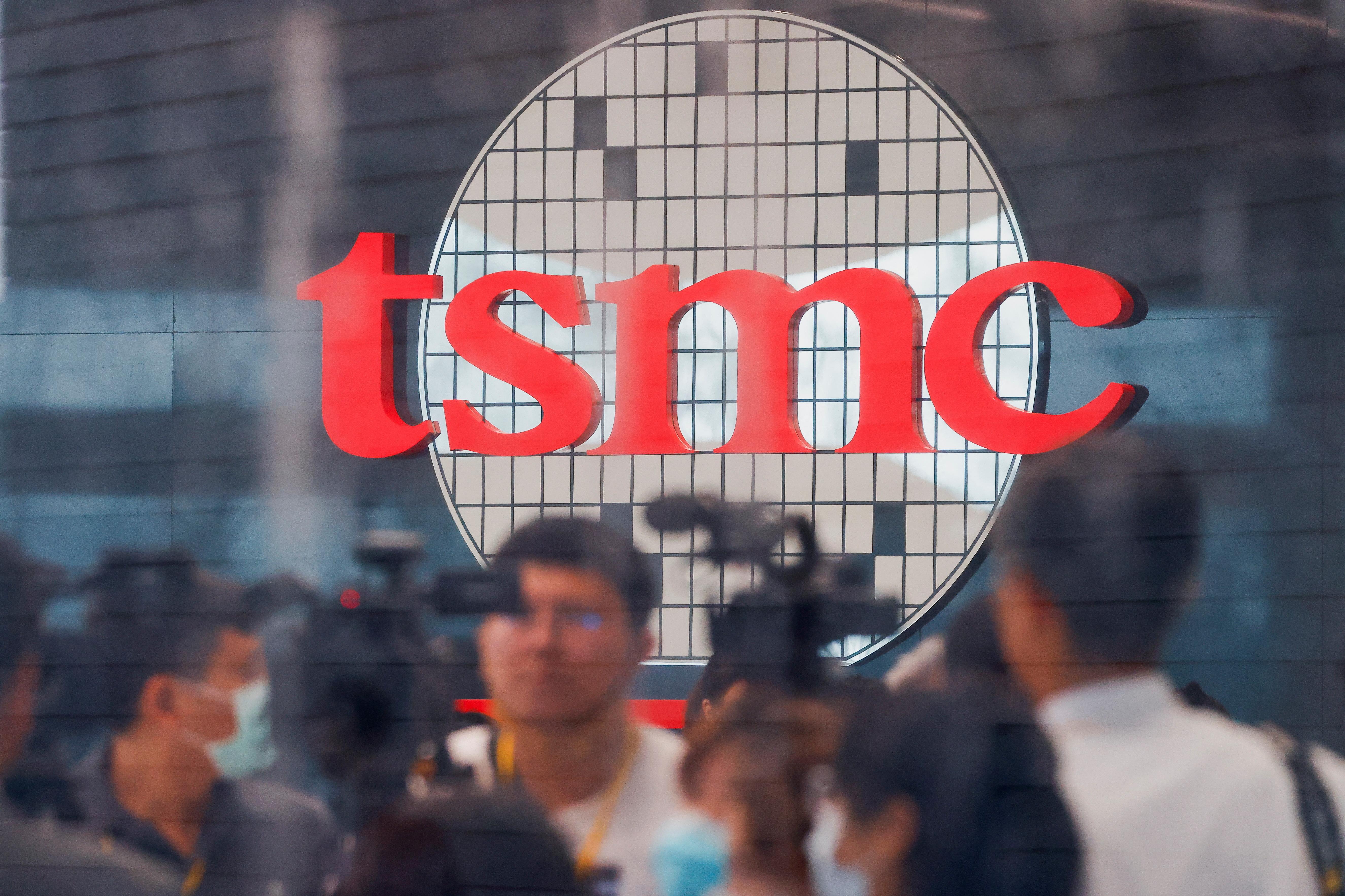
In this context, the global chip foundry leader TSMC announced in the United States, Japan, and Germany, but Taiwan, which has a complete supply chain ecosystem, will still be the base camp of global research and development and manufacturing.TSMC is currently making more than 90 % of the cutting -edge chips worldwide.
According to the annual report of TSMC in 2022, the company's total employees exceeded 73,000, producing 15.3 million pieces of 12 -inch wafers (about 600 chips per piece), and tailoring 1 for 532 customers worldwide.2698 chips.In contrast, the estimated employees and production capacity of all overseas factories do not exceed 20 % of the total.
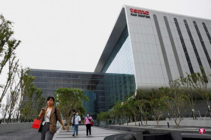
TSMC recently announced a high -profile determination to leave Taiwan, including the global R & D centers that can accommodate 8,000 R & D personnel on July 28. On August 8th, it was announced that it was produced in the most advanced two -nanometer process in Kaohsiung Factory on August 8The chip is planned to be tried in the second half of 2024 and mass production in 2025.According to the existing plan, the overseas factories are behind at least one generation or three years.
One nanometer (NM) is one -million -dollar millimeter (mm). The nail -sized two -nanometer process chip can accommodate more than 50 billion electrical crystals (also known as crystal pipes), which is more power -saving.
However, as the crystals have been slightly smaller than the virus (about 100 nanometers) that are difficult to discern than the naked eye, the semiconductor technology is approaching the physical limit, and it must be found another way to find a breakthrough.
According to the TSMC's annual technical forum on May 11, after entering the two -nanometer process, scientific researchers will adopt vertical stacking crystal architecture, new semiconductor materials, and advanced packaging technology to further reduce the area and improve the area and improveSave power performance.
In the past 20 years, TSMC has begun to double the chip density every two years since the 90 -nanometer process, and the most advanced three -nanometer process is currently.At present, TSMC is preparing to adopt a new crystal architecture to mass -produced a two -nanometer process in 2025, and strives to launch a 1.4 nanometer process chip in 2028.
Faced with a nanometer and more precise chip process, TSMC is studying to make breakthroughs to achieve a more space -saving complementary field effect crystal (CFET) architecture, which is expected to reach the standard at a generation of one generation every three years.It is currently planned to mass -produce one nanometer in 2031. After another three years, I hope to break through the 0.7 nanometer (or seven Emi) process.
According to this newspaper, materials and architectures used in the 1.4 nanometer and below are still open research. At present, 70 % are grasped, but whether it can meet the standards as scheduled is still full of variables.
TSMC is currently strengthening research through advanced packaging technology to connect different functions (including computing, memory, high -frequency signals and power saving) to the same substrate to improve performance and yield.
It is reported that TSMC also actively dominates the cooperation of industrial and academic circles, including promoting the guidance of universities and research institutions at home and abroad to study and use new low -dimensional materials, such as graphene and nano -carbon pipes to accelerate technical research.
Dr. Wu Lingxiang, a technical industry consultant and the CEO of the Science and Technology Think Tank for the technical research of TSMC, pointed out in an interview with Lianhe Morning Post that there are still many future variables.During the process, many scientific believe that impossible is possible.
"It is certain that TSMC is now leading the leader and Samsung situation, but it is still not enough. The key to the United States has been leading in the past 30 years.It's the right direction. "
Huang Shicong, a Taiwan Finance commentator and director of investment consultants, believes that TSMC's advantage lies in the leadership of technology and manufacturing, and won the trust of large customers such as Apple and Nvidia, and has a complete supply chain ecological support in Taiwan.In the future, more materials and equipment manufacturers need to cooperate, especially the EUV manufacturer (ASML), a Dutch manufacturer (ASML), which recently established a R & D center in Taiwan.
Expert analysis: Whether Beijing is not necessary to have a relationship with Taiwan and TSMC
Recently, Liu Deyin, chairman of TSMC, denied in an interview that semiconductor was a reason to block or encourage the mainland to attack Taiwan, and was interpreted as denying that the "Silicon Shield" could protect the Taiwan.Both experts agree that whether Beijing and TSMC have no necessary relationship with TSMC. It also pointed out that once the "silicon shield" becomes "silicon target", it will impact the US and global economy.
Huang Shicong said that the existence of TSMC's survival on the United States is actually much greater than the mainland, because 60 % of TSMC's revenue comes from US businessmen, and the mainland accounts for only about 10 %.Breeding.
Wu Lingxiang said that TSMC announced that Taiwan is also to protect himself and accumulate more chips to face the pressure of other countries, but the issue of Taiwan Strait depends on the strength and willingness of Beijing and Washington.Mainland China ’s willingness to unify Taiwan has never changed, and it will not be shaken by TSMC existence or disappearance.
"If all the factor that launched the war, TSMC is ranked very behind the War Ledger of both sides."